Product Description
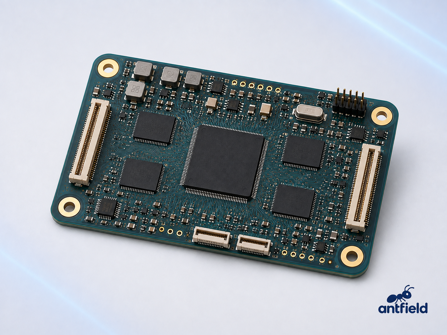
The Antfield FPGA Processing Board is designed forhigh-speed data acquisition, deterministic parallel processing and low-latencyinterface control in robotic systems.
Unlike a conventional processor that executes instructionsmainly in sequence, an FPGA contains programmable logic resources that canprocess multiple data streams simultaneously. This makes the board suitable forrobotic vision, high-speed sensor interfaces, motor-control timing, protocolconversion and other applications requiring predictable response times.
In a robotic vision system, the board can receive datasimultaneously from stereo cameras, depth sensors and other perception devices.It can perform image synchronization, filtering, data formatting and featurepreprocessing before transmitting the processed data to the robot’s maincomputing or AI board.
FPGA resources, memory capacity, high-speed interfaces,power design, PCB dimensions and programmable logic functions can be customizedaccording to project requirements.
Main Functions
Parallel data processing
High-speed sensor-data acquisition
Multi-camera synchronization
Image and depth-data preprocessing
Deterministic low-latency control
Communication-protocol conversion
Encoder and pulse-signal processing
High-speed PWM generation
Motor-control timing support
Custom digital-interface implementation
Hardware-level filtering
Data aggregation and packet formatting
Safety-signal monitoring
Real-time event detection
High-bandwidth data transfer
Applications
Humanoid robot vision systems
Stereo-camera processing
Depth-camera and LiDAR interfaces
Industrial inspection robots
High-speed machine-vision systems
Robotic motor-control systems
Encoder and resolver interfaces
Multi-sensor synchronization
AGV and AMR perception systems
Robot communication gateways
Medical imaging robots
High-speed data-acquisition equipment
Custom robotic control platforms
Main Components
Component | Function |
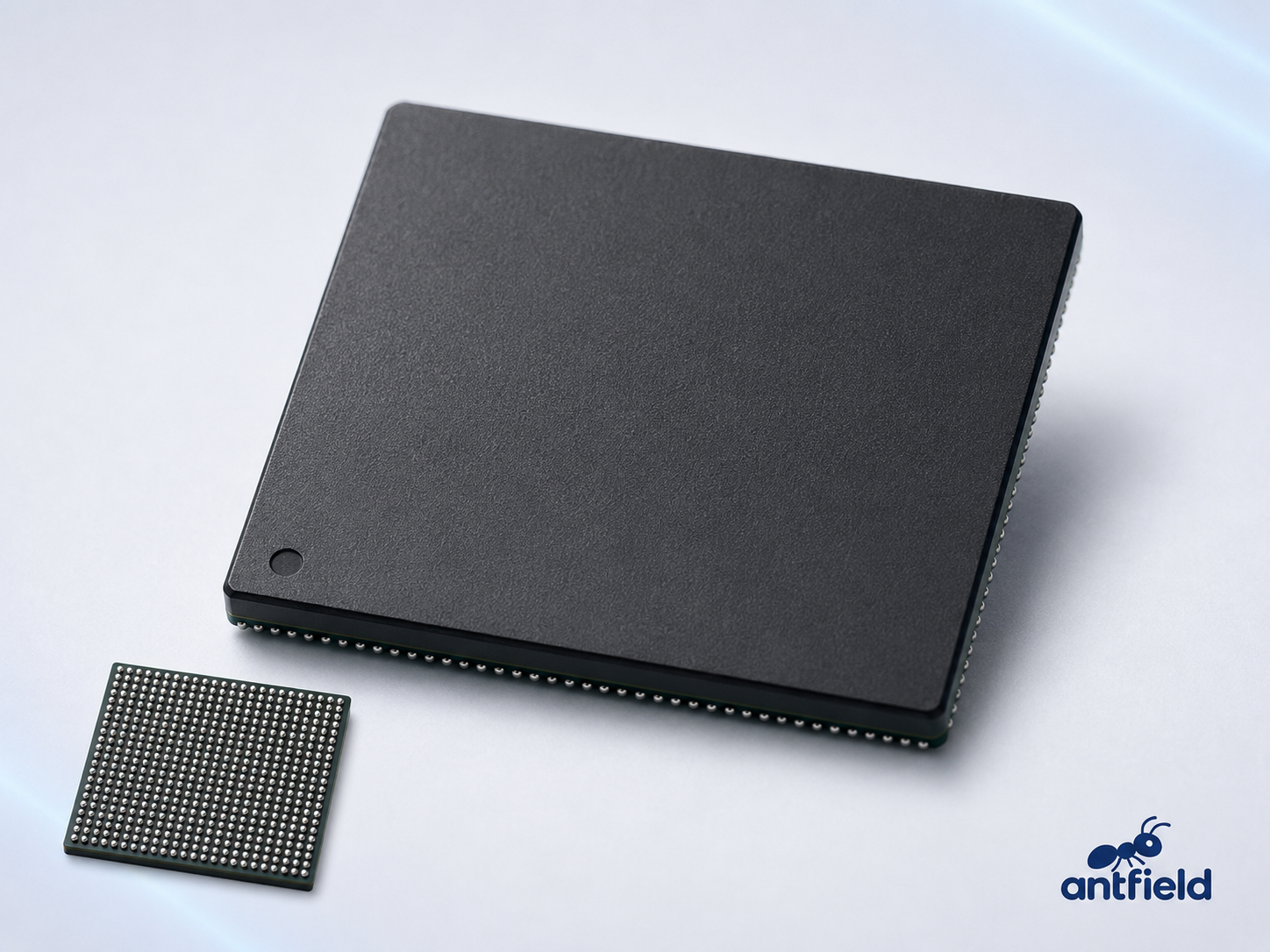
FPGA Device | Implements programmable parallel-processing logic, custom interfaces, timing control and hardware accelerators. |
Programmable Logic Cells | Build custom digital circuits inside the FPGA, including state machines, filters and protocol controllers. |
DSP Blocks | Perform high-speed multiplication, filtering, coordinate calculations and signal-processing operations. |
Block RAM | Provides fast internal memory for buffers, lookup tables, FIFOs and intermediate data. |
High-Speed Transceivers—Optional | Support serial data links such as Ethernet, PCIe or other high-bandwidth interfaces. |
DDR Memory | Stores image frames, depth data and large intermediate datasets that exceed the FPGA’s internal memory. |
Configuration Flash | Stores the FPGA configuration bitstream and loads the hardware design after power-up. |
Clock Oscillator | Provides a stable timing reference for the FPGA, memory and communication circuits. |
Clock Generator or Jitter Cleaner | Generates and distributes multiple low-jitter clock signals required by high-speed interfaces. |
Power-Management ICs | Generate and sequence the different voltages required by the FPGA core, I/O banks, memory and transceivers. |
DC-DC Converters | Efficiently convert the input supply into the board’s main operating voltages. |
Power Inductors | Store energy and filter current in switching power-conversion circuits. |
LDO Regulators | Provide low-noise voltage for sensitive clocks, analog circuits or transceivers. |
Power-Sequencing Circuit | Applies power rails in the correct order to ensure reliable FPGA start-up. |
Ethernet or SERDES PHY—Optional | Provides the physical-layer interface for high-speed communication. |
Camera Interface Connectors | Connect cameras, image sensors and depth sensors to the FPGA board. |
Board-to-Board Connectors | Carry high-speed data, power and control signals between the FPGA board and other robot modules. |
JTAG Header | Supports FPGA programming, configuration, debugging and production testing. |
ESD Protection Components | Protect external communication and sensor interfaces from electrostatic discharge. |
Precision Resistors and Capacitors | Provide termination, impedance matching, power filtering and stable circuit operation. |
PCB and Mounting Holes | Provide high-speed routing, power distribution, grounding, heat spreading and mechanical installation. |
How the FPGA Board Works
The FPGA processing workflow normally includes:
Data acquisition: Multiple cameras, encoders or sensors send data to the FPGA simultaneously.
Synchronization: The FPGA aligns data using precise clocks, triggers and timestamps.
Parallel processing: Multiple logic blocks process different data streams at the same time.
Buffering: Internal RAM or external DDR memory temporarily stores frames and sensor data.
Data output: Processed results are transmitted to the robot’s MCU, MPU or AI computing board.
Real-time control: The FPGA can also generate precise timing, triggers, PWM or interface-control signals.
Typical Robotic Vision Functions
Depending on the programmed logic, the FPGA board canperform:
Camera triggering and synchronization
Image-stream reception
Pixel-format conversion
Image cropping and scaling
Noise filtering
Color-space conversion
Stereo-image alignment
Depth-data synchronization
Feature preprocessing
Data compression or packetization
Timestamp generation
Frame buffering
High-speed data forwarding
The FPGA normally performs deterministic preprocessing andinterface acceleration. High-level object recognition, semantic understandingand autonomous decision-making are usually handled by an MPU, GPU, NPU or AIcomputing board.
FPGA, MCU and MPU Comparison
Device | Main Strength | Typical Robotic Role |
FPGA | Parallel processing and deterministic timing | Vision preprocessing, sensor interfaces and custom hardware acceleration |
MCU | Low-power real-time control | Motor control, sensor acquisition and communication |
MPU | Operating systems and complex applications | Navigation, user interfaces and high-level coordination |
GPU/NPU | Large-scale parallel AI computation | Neural-network inference, recognition and perception |
Many robotic systems combine an FPGA with an MCU or AIprocessor instead of using only one processing device.
Interface Options
Depending on the FPGA and board configuration, the boardcan support:
MIPI CSI-2
LVDS
Parallel camera interface
Gigabit or multi-gigabit Ethernet
PCI Express
USB through an external controller
CAN or CAN FD
RS-485
UART
SPI
I²C
GPIO
PWM
Quadrature encoder input
SSI and BiSS-C
Custom serial or parallel protocols
High-speed interface support must be confirmed using theactual FPGA resources, PHY devices, PCB stack-up and signal-integrity design.
Recommended Specifications
Specification | Description |
FPGA Family and Device | Selected FPGA series and exact device |
Logic Elements | Available programmable logic capacity |
DSP Blocks | Hardware resources for signal processing |
Block RAM | Internal FPGA memory capacity |
High-Speed Transceivers | Number and maximum supported data rate |
DDR Type and Capacity | External memory technology and storage capacity |
Configuration Memory | Flash capacity used for FPGA programming |
Camera Inputs | Number and type of supported camera interfaces |
Maximum Data Rate | Verified input and output bandwidth |
Clock Frequency | Main FPGA and interface clock rates |
Communication Interfaces | Ethernet, PCIe, CAN, RS-485, SPI or other interfaces |
Input Voltage | Required board-level power supply |
Power Consumption | Typical and maximum board consumption |
Operating Temperature | Supported environmental temperature range |
Cooling Method | Passive conduction, heat sink or forced-air cooling |
Programming Interface | JTAG, Flash or remote configuration |
PCB Stack-Up | Number of layers and impedance-control requirements |
Dimensions | PCB length, width and height |
Main Advantages
True parallel hardware processing
Deterministic and predictable latency
Supports multiple simultaneous data streams
Flexible custom-interface implementation
Suitable for high-speed sensor acquisition
Reconfigurable after manufacturing
Precise synchronization and timing control
Hardware acceleration without a full operating system
Scalable logic and memory resources
Customizable interfaces and processing pipelines
Installation Considerations
Provide adequate cooling for the FPGA and power section.
Verify FPGA junction temperature under maximum processing load.
Use controlled-impedance PCB routing for high-speed interfaces.
Keep differential pairs length-matched and properly terminated.
Provide stable, low-noise power for every FPGA voltage rail.
Follow the required power-up and power-down sequence.
Place DDR memory close to the FPGA.
Use low-jitter clocks for cameras and high-speed transceivers.
Separate switching power circuits from sensitive clocks and data links.
Ensure sufficient grounding and shielding for camera cables.
Provide a reliable configuration and recovery method.
Verify signal integrity, power integrity, EMC and thermal performance.
Test the actual programmed logic under maximum data bandwidth.
Important Technical Note
An FPGA is not automatically a complete AI processor. Itsfunction depends on the logic design programmed into it.
The FPGA board can accelerate image processing, sensorfusion interfaces and data movement, but neural-network performance depends on:
Avoid claiming that the board supports a specific AI model,camera resolution, frame rate or communication speed unless it has beenverified using the final hardware and FPGA design.


