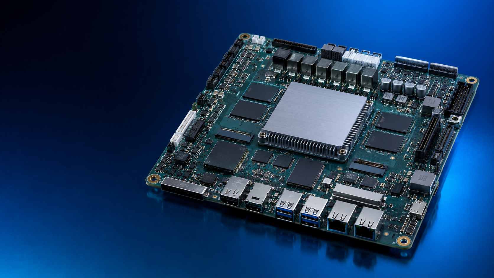
Key Features
Multi-camera synchronization
FPGA/ISP or vision-processor acceleration
High-speed memory and image interfaces
Local inference and sensor fusion
Typical Electronic Components
FPGA, ISP, vision SoC or accelerator; DDR; eMMC/Flash; clock tree; Ethernet/USB/MIPI interfaces; PMIC.
Reference PCB and PCBA Parameters
Reference item | Typical guidance |
Typical layers | 8-16 layers |
Material | High-Tg FR-4 or low-loss laminate |
Density | HDI, microvias and via-in-pad |
High-speed buses | DDR, MIPI, PCIe, USB and Ethernet |
Thermal | Heat spreader, sink and airflow as required |
Testing | Memory, video pipeline, interface and thermal test |
Manufacturing and Engineering Priorities
Plan stack-up around BGA escape, DDR and high-speed interfaces.
Control clock integrity, power sequencing and rail ripple.
Budget bandwidth across cameras, memory and network interfaces.
Provide an engineered thermal path for processor and memory hot spots.
Design and Commercial Cautions
Algorithm performance is separate from bare-PCB capability.
Define camera count, resolution, frame rate and latency before hardware selection. Use 3D X-ray for hidden high-density solder joints.
|
Applications
Industrial inspection, autonomous navigation, picking, recognition and visual SLAM.

